- 您现在的位置:买卖IC网 > Sheet目录3877 > PIC18F13K50-I/MQ (Microchip Technology)IC PIC MCU FLASH 512KX8 20-QFN
PIC18F1XK50/PIC18LF1XK50
DS41350E-page 12
Preliminary
2010 Microchip Technology Inc.
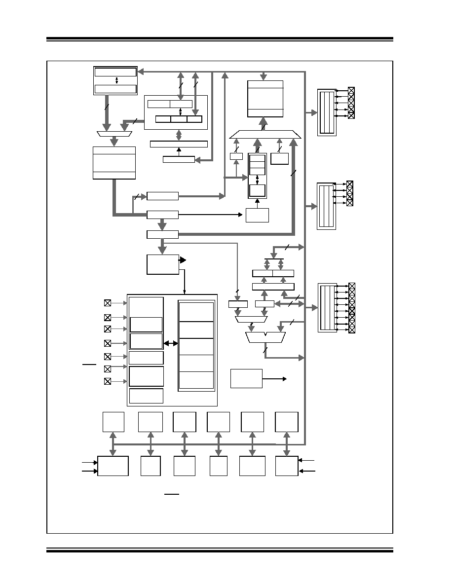
FIGURE 1-1:
PIC18F/LF1XK50 BLOCK DIAGRAM
Instruction
Decode and
Control
PORTA
PORTB
PORTC
RA1
RA0
Data Latch
Data Memory
Address Latch
Data Address<12>
12
Access
BSR
FSR0
FSR1
FSR2
inc/dec
logic
Address
4
12
4
PCH
PCL
PCLATH
8
31-Level Stack
Program Counter
PRODL
PRODH
8 x 8 Multiply
8
BITOP
8
ALU<8>
20
8
Table Pointer<21>
inc/dec logic
21
8
Data Bus<8>
Table Latch
8
IR
12
3
ROM Latch
PCLATU
PCU
Note
1:
RA3 is only available when MCLR functionality is disabled.
2:
OSC1/CLKIN and OSC2/CLKOUT are only available in select oscillator modes and when these pins are not being used
as digital I/O. Refer to Section 2.0 “Oscillator Module” for additional information.
3:
PIC18F13K50/PIC18F14K50 only.
EUSART
Comparator
MSSP
10-bit
ADC
Timer2
Timer1
Timer3
Timer0
ECCP1
BOR
Data
EEPROM
W
Instruction Bus <16>
STKPTR
Bank
8
State machine
control signals
Decode
8
Power-up
Timer
Oscillator
Start-up Timer
Power-on
Reset
Watchdog
Timer
OSC1(2)
OSC2(2)
VDD,
Internal
Oscillator
Fail-Safe
Clock Monitor
Precision
Reference
Band Gap
VSS
MCLR(1)
Block
LFINTOSC
Oscillator
16 MHz
Oscillator
Single-Supply
Programming
T1OSO
T1OSI
FVR
CVREF
Address Latch
Program Memory
Data Latch
CVREF
RA3
RA4
RA5
RB4
RB5
RB6
RB7
RC0
RC1
RC2
RC3
RC4
RC5
RC6
RC7
(512/768 bytes)
VUSB
USB
Module
USB
LDO(3)
Regulator
发布紧急采购,3分钟左右您将得到回复。
相关PDF资料
PIC16F1934-I/PT
IC PIC MCU FLASH 256KX7 44-TQFP
PIC24F16KL402-I/SS
IC MCU 16BIT 16KB FLASH 28-SSOP
PIC16LF1934-I/PT
IC PIC MCU FLASH 256KX7 44-TQFP
PIC16C58B-20/P
IC MCU OTP 2KX12 18DIP
PIC18F24K20-I/SP
IC PIC MCU FLASH 8KX16 28-DIP
PIC16F1936-I/SP
IC PIC MCU FLASH 512KX14 28SPDIP
PIC18F43K20-I/PT
IC PIC MCU FLASH 4KX16 44-TQFP
PIC16F627A-I/SS
IC MCU FLASH 1KX14 EEPROM 20SSOP
相关代理商/技术参数
PIC18F13K50-I/P
功能描述:8位微控制器 -MCU 8KB Flash 512 RAM 15 I/O 10-B ADC USB 2.0 RoHS:否 制造商:Silicon Labs 核心:8051 处理器系列:C8051F39x 数据总线宽度:8 bit 最大时钟频率:50 MHz 程序存储器大小:16 KB 数据 RAM 大小:1 KB 片上 ADC:Yes 工作电源电压:1.8 V to 3.6 V 工作温度范围:- 40 C to + 105 C 封装 / 箱体:QFN-20 安装风格:SMD/SMT
PIC18F13K50-I/P
制造商:Microchip Technology Inc 功能描述:20 Pin 8 KB Flash 512 RAM 15 I/O 10
PIC18F13K50-I/SO
功能描述:8位微控制器 -MCU 8KB Flash 512 RAM 15 I/O 10-B ADC USB 2.0 RoHS:否 制造商:Silicon Labs 核心:8051 处理器系列:C8051F39x 数据总线宽度:8 bit 最大时钟频率:50 MHz 程序存储器大小:16 KB 数据 RAM 大小:1 KB 片上 ADC:Yes 工作电源电压:1.8 V to 3.6 V 工作温度范围:- 40 C to + 105 C 封装 / 箱体:QFN-20 安装风格:SMD/SMT
PIC18F13K50-I/SO
制造商:Microchip Technology Inc 功能描述:20 Pin 8 KB Flash 512 RAM 15 I/O 10
PIC18F13K50-I/SS
功能描述:8位微控制器 -MCU 8KB Flash 512 RAM 15 I/O 10-B ADC USB 2.0 RoHS:否 制造商:Silicon Labs 核心:8051 处理器系列:C8051F39x 数据总线宽度:8 bit 最大时钟频率:50 MHz 程序存储器大小:16 KB 数据 RAM 大小:1 KB 片上 ADC:Yes 工作电源电压:1.8 V to 3.6 V 工作温度范围:- 40 C to + 105 C 封装 / 箱体:QFN-20 安装风格:SMD/SMT
PIC18F13K50-I/SS
制造商:Microchip Technology Inc 功能描述:8-Bit Microcontroller IC
PIC18F13K50T-I/SO
功能描述:8位微控制器 -MCU 8KB Flash 512 RAM 15 I/O 10-B ADC USB 2.0 RoHS:否 制造商:Silicon Labs 核心:8051 处理器系列:C8051F39x 数据总线宽度:8 bit 最大时钟频率:50 MHz 程序存储器大小:16 KB 数据 RAM 大小:1 KB 片上 ADC:Yes 工作电源电压:1.8 V to 3.6 V 工作温度范围:- 40 C to + 105 C 封装 / 箱体:QFN-20 安装风格:SMD/SMT
PIC18F13K50T-I/SS
功能描述:8位微控制器 -MCU 8KB Flash 512 RAM 15 I/O 10-B ADC USB 2.0 RoHS:否 制造商:Silicon Labs 核心:8051 处理器系列:C8051F39x 数据总线宽度:8 bit 最大时钟频率:50 MHz 程序存储器大小:16 KB 数据 RAM 大小:1 KB 片上 ADC:Yes 工作电源电压:1.8 V to 3.6 V 工作温度范围:- 40 C to + 105 C 封装 / 箱体:QFN-20 安装风格:SMD/SMT